They described the device this week at ISSCC in San Francisco.
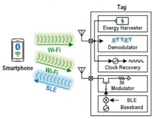
The tag has two antennas, both of which are used to extract power from the incoming Wi-Fi field. One also receives Wi-Fi (802.11b) signals for decoding and clock recovery, and the other handles Bluetooth using frequency division duplex communication.
Bluetooth transmitted energy is backscattered from the Wi-Fi field by appropriately modulating a 50Ω load on the Bluetooth antenna. According to the team, the necessary phase compensation was demonstrated for the first time in this project.
Internally, the received Wi-Fi signal is reprocessed using a new “phase flip” tracking technique to demodulate the DBPSK Wi-Fi signal, provide a clean CW carrier signal for Bluetooth signal generation, and Adopts an injection lock ring oscillator to achieve a stable 8MHz system clock.
The IC is manufactured in a 65nm CMOS process and occupies 0.95mm.2.
Both downlink and uplink operate at 1Mbit/s and the maximum system power is 17μW.
The prototype used Wi-Fi Ch7 (2.442GHz) energy to transmit data on BLE Ch39 2.48GHz.
ISSCC24 Paper 23.3 Passive crystalless Wi-Fi-to-BLE tag demonstrating battery-free FDD communication with a smartphone.


