Wireless communication systems have seen an exponential development in recent years, and this scenario leads to continue with highly demanded of sophisticated technologies. For instant, higher transmission data rate and shorter latency with increment in channel capacity are the critical parameters that must be improved significantly to satisfy the requirement of future mid-band fifth-generation (5G) wireless systems below 6 GHz. For this, massive MIMO technology is one of the potential solutions1,2,3, which can simultaneously support more users, offers improved diversity, and multiplexing, as well as enables a significant enhancement in energy-efficient systems. Massive MIMO operation has been studied widely based on homogeneous arrays and omnidirectional patterns4,5,6. However, the influence of the directional antenna gain pattern on the performance of mMIMO system has been neglected in most of these studies.
5G MIMO antenna systems have been reported for either the single or dual operational bands7,8,9. Recently, three working bands of 5G New Radio (NR) have been started by Generation Partnership Project (3GPP)10; these bands inholding the mid-band application at a span range of (3.3–3.8 GHz), (3.3–4.2 GHz), and (4.4–5.0 GHz) which represent N78, N77 and N79 respectively. Besides, every country can choose its own 5G demanded bands, as mentioned above. For instant, China has been officially declared to utilize two bands at (3.3–3.6 GHz) and (4.8–5.0 GHz)11, although the frequency band from 3.4 to 3.8 GHz has been decided by European Union (EU) for the 5G application12. Consequently, to cover the aforementioned 5G operating bands for mobility reasons, a specific MIMO antenna system must be developed to cover the desired 5G N77/N78/N79 bands, which is not addressed by the designs proposed in Refs.13,14.
Designing MIMO antennas with high isolation between elements of the antenna, low cost, less usage of energy, small size, and being lightweight is often a challenging task. However, one of the drawbacks of antenna performance is the narrow bandwidth, which restricts the usage of new wireless systems. To avoid these challenges, several methods have been sophisticated recently. For example, the reactive impedance surface (RIS) method15 can be used to improve antenna radiation and bandwidth characteristics by tuning the RIS between electric (PEC) and magnetic (PMC) conductors and surfaces. In addition, the overall antenna size can be reduced. The antenna performance is greatly improved in Ref.16 by using a two-dimensional left-handed metamaterial (LHM) design on the dielectric substrate’s top (patch) and bottom (ground) sides. This method generates capacitive-inductive features due to the coupling between the designed patch and bottom plane configuration, which creates a backward traveling wave. However, a periodic structure on the ground plan is applied for a passive antenna before testing for temperature sensing, as offered in Ref.17. These bottom based surface layers allow a considerable improvement in the antenna size and bandwidth characteristics.
Metamaterial (MTM), as an artificial medium, has several unusual features, such as negative (refractive index, permeability, and permittivity), making it appropriate for a variety of applications, including absorber18, bio sensing19, microwave imaging20, antennas21, metamaterial coding22, metamaterial lensing23, terahertz metamaterial24, and microwave devices like GPS5, WiMAX25.
In Ref.26, there is a negative index metamaterial made up of extended beams enclosed to a plate. A 3 dimensions acoustic MTM is examined in Ref.27 which can be used to create a bandgap at the location of deep sound attenuation which can be employed as an acoustic filter for noise cancellation. All of these metamaterials’ features have appeared at specified frequency bands of interest, dependent on the geometrical arrangement in the array and the structure’s fixed composition. As a result, there is a growing interest in MTMs that emphasize numerous operating frequencies that are tuned by diverse stimuli such as electrical, mechanical, or optical signals. In addition, certain MTMs and resonators for diverse applications and property analyses are described in Ref.28. In Ref.29, a hexagonal Gap coupled split-ring resonator-based MTM with a size of 10 × 10 mm2 that covers the S and X bands is described. MTM with a concentric ring-based resonator, on the other hand, is demonstrated in Ref.30, which demonstrates a single negative characteristic with dual resonances at 13.9 GHz and 27.5 GHz to improve the microstrip transmission line performance. In Ref.31, a triple-band response is reported for an open delta shaped ENG MTM. Furthermore, for microwave applications at S, C, and X-band, a pi-shaped complementary split-ring resonator (CSRR) associated with metal inclusion is created and described in Ref.32.
MTM unit cell was verified to increase antennas’ performance in terms of gain, isolation, bandwidth, radiation patterns, …etc. due to its ability to perturb the current distribution patch along with the antenna radiator. In contrast, negative real value properties have occurred on the achieved refractive index (NRI) as well as both permeability (µ) and permittivity (ɛ)33,34. However, a MTM with a near-zero refractive index (NZRI) characteristic has been studied to improve the overall performance of the antenna in specific bands, including S, C, and X bands35. In addition, various types of MTMs are used to minimize the coupling between array elements36,37. However, the previously suggested decoupling approaches are difficult to build and operate on miniaturize MIMO antenna elements. Unlike conventional antenna arrays, this research uses a series of small split-ring resonators (SRRs) as resonators and to increase the isolation between the antenna elements.
Few works offered a MIMO configuration without an array mode by using multimode at each element (beamsteering). Reference38 dispersed 108 elements along a nine-faced polyhedron ring operating at 2.4 GHz. This was accomplished by utilizing a developed patch to produce three modes per element: first (bandwidth of 238 MHz), second (254 MHz) modes have around 6.5 dBi gain, while the third mode of 102 MHz bandwidth has a gain of 1.21 dBi. Manteuffel and Martens39, on the other hand, adopted a sheet to accommodate four modes which covered a wide spectrum from 6 to 8.5 GHz, as well as an 11 × 11 array. With a very low envelope correlation coefficient, the port isolation was greater than 20 dB.
In this paper, quite high-isolation massive MIMO antenna with 32 elements that can cover 3400–3650 MHz is proposed for a future 5G base station with a measured bandwidth of 250 MHz. In addition, an analysis of a unique ENG/NZRI/DNG metamaterial unit cell is conducted to support the proposed design’s operational working principle, which is based on the epsilon negative and near-zero refractive index properties, which are designed to simultaneously improve the isolation and overall performance of the MIMO antenna system. Four compact square-shaped splatted parts make up the proposed MTM. In contrast to traditional isolation solutions, the proposed MTM-based technology allows for substantial decoupling of up to 32 dB between the proposed radiating MIMO antenna elements and small array elements with ECC 0.0001. The experimental data and the findings from the CST microwave studio have been compared, and they exhibit great agreement, demonstrating the precision of the proposed MTM, subarray, and MIMO antennas. The suggested antenna has a fractional BW of roughly 7.1% and has negligible mutual coupling. Table 1 compares the proposed MIMO antenna loaded with the proposed unique MTM to other antennas previously reported in the literature.
Design of metamaterial unit cell
Figure 1a shows the schematic view of the proposed ENG metamaterial unit cell along with its geometrical configuration parameters. It is composed of four low profile square split-ring resonators (SSRR) combined by an electrical 0.5 mm width slab and printed on the front side of Rogers 5880 substrate with a thickness of 1.575 mm, a dielectric constant εr of 2.2 and loss tangent δ of 0.0009. The proposed ENG metamaterial includes two symmetrical crescent shaped SSRR with a middle split portion on the upper arms, whereas the other two are splitted on the corner of either right or left SSRR arms. An array prototype of 1 × 3 unit cells is shown in Fig. 1b. It is created on top of the same substrate at vertical x axis-direction with 0.5 mm distance between each two units. Figure 1c characterizes the electromagnetic simulated wave propagation of the suggested ENG-DNG metamaterial design in the z-direction wherever it was positioned between 2 waveguide ports. Both perfect electric and perfect magnetic conductors (PEC, PMC) boundary conditions were applied to x-axis, and y-axis respectively. Furthermore, x-direction is also chosen to simulate the proposed MTM whereas PEC and PMC boundary conditions were utilized at z-axis, and y-axis respectively as shown in Fig. 1d.
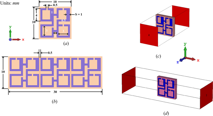
The proposed metamaterial unit cell structure: (a) unit cell geometry, (b) 3 × 1 MTM unit cell array, (c), simulation set up in z-axis, (d) simulation set up in x-axis.
Using the normal incidences data of scattering parameters, a robust approach is used to obtain the valuable metamaterial parameters46. The transmission (S21) and reflection coefficients (S11) of the designed MTM unit cell are first evaluated using simulations in the frequency span from 2 to 4 GHz. Using an Agilent N5227 PNA Microwave Network Analyzer with waveguides to co-axial adapters, the S-parameters of the proposed MTM unit cell are extracted. For the appropriate frequency range, a SAR-1834031432-KF-S2-DR (1–18 GHz) waveguide was employed, and the MTM fabricated prototype has been arranged for measurements purpose between two waveguides at z-axis directions, as illustrated in Fig. 2.
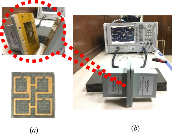
Metamaterial experimental setup: (a) measurement of MTM S-parameters, (b) unit cell with Horn antenna.
Metamaterial unit cell working principle
For more understanding of the physical MTM phenomena in both electric and magnetic field zones, the surface current distribution of two selected frequencies is investigated. Figure 3a,b illustrate the suggested unit cell MTM surface current distributions at 3.4 and 3.5 GHz, respectively. The surface current density is declared by colors, whereas the arrows denote the direction of surface current distribution.
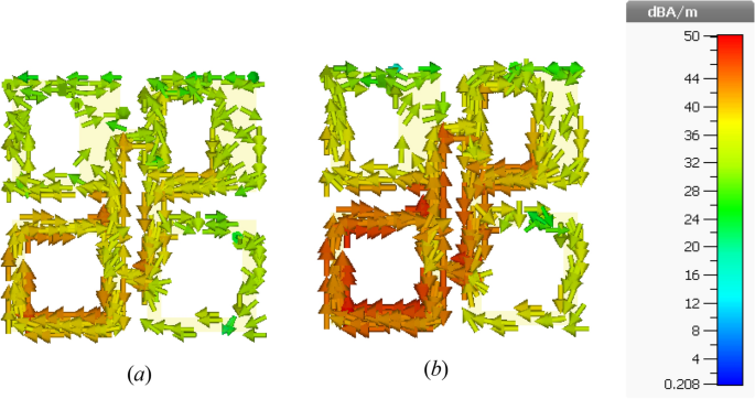
Unit cell surface current distribution at (a) 3.4 GHz, (b) 3.5 GHz.
At 3.4 GHz, a noticeable surface current can be seen, as shown in Fig. 3a. On the inner edge of the left bottom square-shaped part, though, the surface current is further strong and intense. Furthermore, the overall MTM unit cell structure perturbs the surface current. Although, once the current flows, opposite side orientations of the noticeable current distribution of MTM-shaped etching strips are seen, nullifying the current and forming a stopband. Though, more concentrated surface current can be clearly detected at 3.5 GHz in Fig. 3b, particularly surrounding the SSR junction, which perturbed the overall structure of the unit cell. The measured S-parameters (S21 and S11) results as well as the simulated results at z-direction are demonstrated in Fig. 4. Its illustrations show that the frequency band at the span of (3.4–3.65 GHz) is a part of the S-band and covers the mid-band of the 5G application. All split square-shaped resonators integrated with the strip line arms are considered the appropriate cause of the realized stopband operational band.
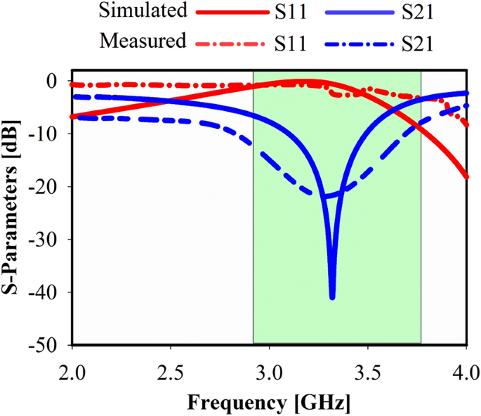
Metamaterial (MTM) s-parameters at the z-axis: measured and simulated.
Figure 5 shows the proposed effective parameters values of MTM. For various MTM unit cell and array configurations, these characteristics involve effective real values and imaginary parts of the realized permeability, refractive index, impedance, and permittivity. The negative indexed region for Epsilon-negative metamaterial (ENG) and near-zero refractive index metamaterial (NZRI) metamaterial is emphasized with light green color in all diagrams. An extensive negative real value of permittivity is achieved with more than 1 GHz bandwidth, as shown in Fig. 5a. Nevertheless, a NZRI property exhibits in the range of (3.1–4.2 GHz) at z-axis wave propagation, as shown in Fig. 5c. Hence, this frequency resonance band can be used for electromagnetic cloaking, high isolation, and high gain antenna design.
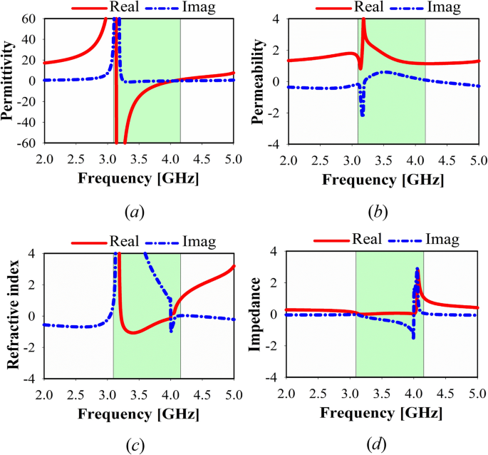
MTM, simulated results at z-axis of 1 × 1 unit cell: (a) permittivity, (b) permeability, (c) refractive index, (d) impedance.
In the z-direction, Fig. 6 illustrates the simulated relative permittivity and refractive index for the various MTM of the 1 × 1, and 1 × 3 array structures. Using one or three array unit cells, similar findings were obtained over a wide frequency range of 3–4.2 GHz. On the other hand, double negative refractive index (DNG) has been achieved along with x-axis in the frequency band (3.49–3.62 GHz) as shown in Fig. 7.
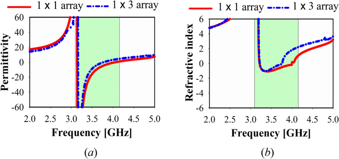
MTM, simulated results of 3 × 3 unit cell: (a) refractive index, (b) permittivity.
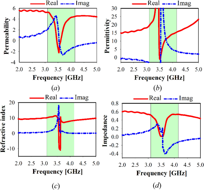
MTM, simulated results at x-axis of 1 × 1 unit cell: (a) permittivity, (b) permeability, (c) refractive index, (d) impedance.
Design of mMIMO antenna system
A subarray designed configuration consists of 2 × 2 patches feeding by a single port built on two dielectric layers of the printed circuit board (PCB), including three copper-clad laminate layers. The top layer is used for the printed patch elements. The developed feeding network (FN) is located at the bottom layer with small partial ground. The middle layer will act as an inclusive reference for both feeding network and antenna patches. Besides, 1.28 mm diameter vias are used as a probe feeding between FN and radiator elements as well as to connect both partial and full ground planes. The substrates used are Rogers 5880 with 2.2 dielectric constant, 1.575 mm thickness, and 0.0009 loss tangent. Figure 8 shows the stackup of the board design. Figure 9a,b illustrate the top and bottom layers of the single-port subarray.
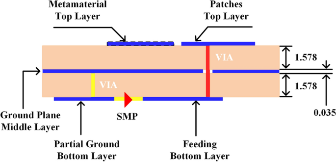
Stackup of the PCB board design displaying the layers.
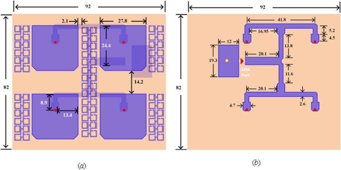
Single port (subarray), (a) top layer with 2 × 2 patches, (b) bottom layer with feeding network (all dimensions are in mm).
The broadband side of the 8-port (32 elements) mMIMO antenna system loaded with MTM is displayed in Fig. 10. Furthermore, a 32 elements mMIMO antenna prototype is fabricated, as demonstrated in Fig. 11.
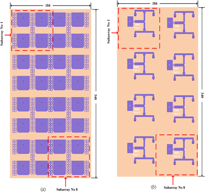
(a) Top view of a single side array, (b) single side array bottom layer.
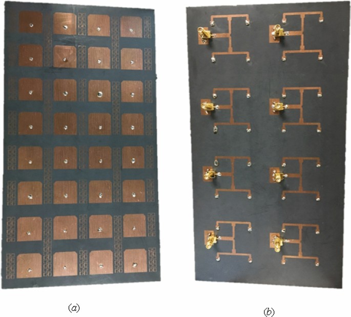
(a) Top view, (b) bottom view of fabricated single-side prototype.


